

How To Draw One Bank Of A 32-byte System
Embedded Systems - Registers Bank/Stack
The 8051 microcontroller has a full of 128 bytes of RAM. Nosotros will discuss most the allocation of these 128 bytes of RAM and examine their usage as stack and register.
RAM Memory Infinite Allocation in 8051
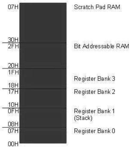
The 128 bytes of RAM inside the 8051 are assigned the address 00 to 7FH. They can be accessed directly as memory locations and are divided into three dissimilar groups as follows −
-
32 bytes from 00H to 1FH locations are set bated for register banks and the stack.
-
sixteen bytes from 20H to 2FH locations are set aside for bit-addressable read/write retention.
-
lxxx bytes from 30H to 7FH locations are used for read and write storage; information technology is chosen every bit scratch pad. These eighty locations RAM are widely used for the purpose of storing information and parameters by 8051 programmers.
Register Banks in 8051
A total of 32 bytes of RAM are prepare aside for the annals banks and the stack. These 32 bytes are divided into four register banks in which each bank has 8 registers, R0–R7. RAM locations from 0 to 7 are ready aside for bank 0 of R0–R7 where R0 is RAM location 0, R1 is RAM location 1, R2 is location ii, and then on, until the retentivity location 7, which belongs to R7 of bank 0.
The 2d bank of registers R0–R7 starts at RAM location 08 and goes to locations OFH. The tertiary banking concern of R0–R7 starts at memory location 10H and goes to location to 17H. Finally, RAM locations 18H to 1FH are set aside for the fourth bank of R0–R7.
Default Register Bank
If RAM locations 00–1F are ready bated for the four registers banks, which annals bank of R0–R7 do nosotros take access to when the 8051 is powered upwardly? The answer is register banking company 0; that is, RAM locations from 0 to 7 are accessed with the names R0 to R7 when programming the 8051. Because it is much easier to refer these RAM locations by names such as R0 to R7, rather than by their memory locations.
How to Switch Annals Banks
Register bank 0 is the default when the 8051 is powered upwardly. Nosotros can switch to the other banks using PSW register. D4 and D3 bits of the PSW are used to select the desired register depository financial institution, since they can be accessed by the bit addressable instructions SETB and CLR. For example, "SETB PSW.3" will set PSW.iii = 1 and select the depository financial institution register 1.
| RS1 | RS2 | Banking company Selected |
|---|---|---|
| 0 | 0 | Bank0 |
| 0 | 1 | Bank1 |
| 1 | 0 | Bank2 |
| ane | 1 | Bank3 |
Stack and its Operations
Stack in the 8051
The stack is a section of a RAM used by the CPU to store information such as information or retention accost on temporary basis. The CPU needs this storage area because express number of registers.
How Stacks are Accessed
As the stack is a section of a RAM, at that place are registers inside the CPU to betoken to it. The register used to access the stack is known as the stack pointer register. The stack arrow in the 8051 is 8-bits broad, and it can take a value of 00 to FFH. When the 8051 is initialized, the SP register contains the value 07H. This means that the RAM location 08 is the first location used for the stack. The storing performance of a CPU register in the stack is known as a PUSH, and getting the contents from the stack back into a CPU register is called a Pop.
Pushing into the Stack
In the 8051, the stack arrow (SP) points to the last used location of the stack. When information is pushed onto the stack, the stack arrow (SP) is incremented by 1. When PUSH is executed, the contents of the annals are saved on the stack and SP is incremented by 1. To button the registers onto the stack, we must utilise their RAM addresses. For instance, the instruction "PUSH 1" pushes annals R1 onto the stack.
Popping from the Stack
Popping the contents of the stack back into a given register is the opposite to the process of pushing. With every popular performance, the top byte of the stack is copied to the annals specified by the instruction and the stack arrow is decremented one time.
Useful Video Courses

Video

Video

Video

Video

Video

Video

Source: https://www.tutorialspoint.com/embedded_systems/es_register_bank.htm
Posted by: brownveng1944.blogspot.com
0 Response to "How To Draw One Bank Of A 32-byte System"
Post a Comment